New Batch Starts Soon ⏰

Become Industry-Ready in 6 Months

Advanced VLSI Design Course in Bangalore

Learn ASIC Design, RTL Verification, FPGA Prototyping & SystemVerilog from expert trainers at Ramaiah Academy. 100% hands-on, tool-driven VLSI training.

4.5

5 LPA

Median
Salary

Hiring Partners

Tools Used

Why choose Ramaiah Academy for VLSI Course?

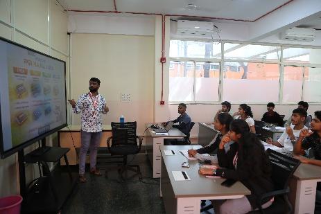
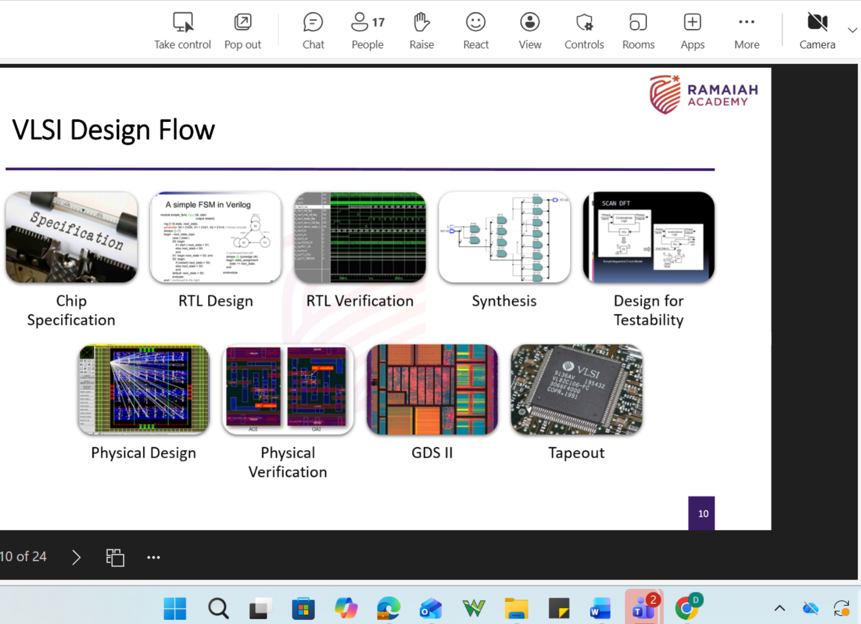
Industry-Oriented Curriculum

The Advanced VLSI program is structured around real industry needs, covering Digital Design, Verilog, System Verilog, UVM, TCL / Python Scripting, Physical Design and Verification, Analog Layout, FPGA Design and Implementation.

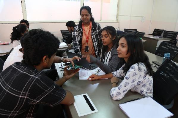
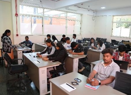
Hands-On Project-Based Learning

Learn through practical, real-world projects using Basys-3, Zedboard, DE-10 Lite, DE-10 Nano, Xilinx Vivado, Quartus, Synopsys and Cadence tools.

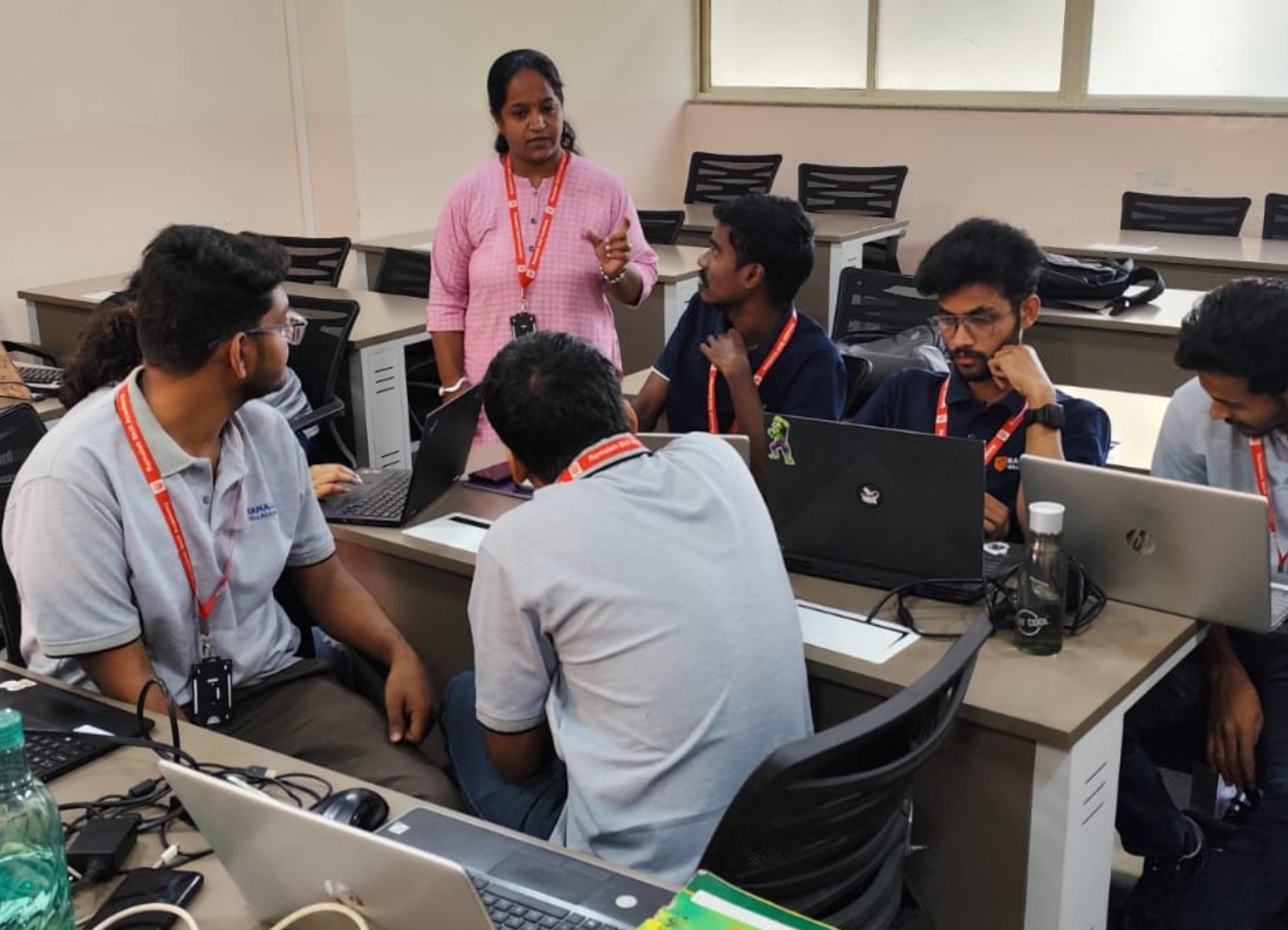
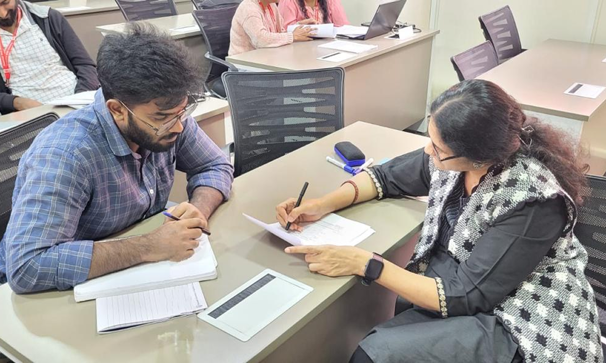
20+ Years of Training Excellence

Backed by the Ramaiah legacy, the academy has over two decades of experience in upskilling engineers with high-quality, job-focused training programs.

Trusted by Leading Companies

Top Companies trust Ramaiah Academy for technical training and talent development.

VLSI Training Programs

Advanced Analog
Layout Design
6 Month
ASIC RTL
Design and Verification
6 Month
Physical
Design and Verification
6 Month
ASIC Prototyping
On FPGA
4 Month
FPGA Implementation
With Verilog HDL
1 Month
RTL Verification
Using System Verilog
1 Month

Advanced Analog Layout Design

Duration: 6 Month · Level: Comprehensive

Intensive program for engineers aiming to master precision analog layout techniques, matching, parasitics, and tape-out-ready designs.

Foundation

  • Linux Essentials
  • Python Scripting
  • TCL Scripting
  • Digital Electronics
  • High Speed Digital Design
  • Circuit Theory
  • Network Theory
  • Introduction to VLSI Design

Advanced Microelectronics

  • Analog Electronics
  • MOSFET
  • Emerging MOS devices – CFET, GAA, FINFET
  • SOI (Silicon-on-Insulator) Technology
  • FD-SOI vs Bulk CMOS
  • Advanced CMOS Nodes (5nm, 3nm, 2nm)
  • Process Variations & Reliability Analysis
  • Layout dependent effects – WPE, PPE, LOD
  • Noise mitigation techniques
  • Introduction to PDK tools & Analog Circuit Simulation
  • Analysis – AC, DC, Transient, Stability

Advanced Analog Circuit Design

  • FINFET Fabrication Process
  • Library Development
  • Library Migration
  • Passive Component Design
  • Op-amp Design Based on FINFET
  • Low Noise Amplifier (LNA) Design
  • Switched Capacitor Circuits
  • Current Mirrors
  • Data Converters – ADC, DAC
  • Voltage Regulators – LDO
  • Phase Locked Loop (PLL)
  • Bandgap Reference & PTAT Circuits
  • Clock and Data Recovery Circuits (CDR)
  • 3D ICs, Heterogeneous Integration and Chiplets
  • Pre-layout & Post-layout Simulations

Layout Design

  • Custom Layout Techniques
  • Matching Techniques
  • Inter-Digitization Techniques
  • RC Balancing Techniques
  • Parasitic Extraction & Optimization
  • Analog IP Macro Development & Testing
  • Overview of Design & Layout Flow
  • Advanced Physical Verification – DRC, LVS, Antenna Checks, DFM
  • Layout Design for Advanced Analog Circuits

Program Takeaways and Support

Apply Now

Why learn with us?

20+ years of training & placement legacy

Internship and Skill Enhancement Certification

Mentorship from real semiconductor professionals

Practical hands-on learning with EDA tools

Real-time projects + internship

Placement support and career guidance

VTU Approved Internship Provider

Hands on Case Study & Projects

Transform theoretical knowledge into real-world skills by building projects under expert guidance. Here are some of the projects you will work on.

Digital voting system with Real Time Authentication and Real Time Result Display

High Performance SPI Master/Slave using Flexible clock and Data Frame Control

Design and Implementation of Reconfigurable Serial Communication Protocol Controller

Design and Verification of AXI4-Lite (Advanced eXtensible Interface) Protocol

Experience Our State-of-the-Art VLSI Lab

Our curriculum is fully hands-on with access to industry-grade tools, FPGA kits, and high-performance systems. Students practise real workflows used in semiconductor companies.

Learn By Doing

Applied Learning Approach

1:1 Mentor Support

Technical Group Discussion

Highly Qualified Faculties

24x7 Online Support

MEET YOUR
VLSI Design FACULTY

Learn from Experienced VLSI Trainers in Bangalore

Priyanka C

Darshan M R

Indicative Placements

Salary

3 LPA

Placed at

Bachanakallappa L

Design and Develeopment Engineer

Salary

3.6 LPA

Placed at

G. Ajaykanth Yadav

Firm Engineer

Salary

3.6 LPA

Placed at

Thanush Kumar B N

Firm Engineer

Placement Assistance

Dedicated career mentors to guide you through applications & interviews.

  • Resume Building
  • Mock Interviews
  • Job Referrals
  • Career Growth Roadmap
career support

90% of our learners who complete the program
land a job within 6 months

Apply Now

Training Programs Offered Under VLSI Design

Program Name Commencement Duration Enroll
Advanced Analog Layout Design Jan 2026 6 Month ENROLL NOW
ASIC RTL Design and Verification Jan 2026 6 Month ENROLL NOW
Physical Design and Verification Jan 2026 6 Month ENROLL NOW
ASIC Prototyping on FPGA Jan 2026 4 Month ENROLL NOW
FPGA Implementation with Verilog HDL Jan 2026 1 Month ENROLL NOW
RTL Verification using System Verilog Jan 2026 1 Month ENROLL NOW

* The duration of our outcome-based Program may vary depending on the learner's pace and progress.

Frequently Asked Questions

Can't find the answer you're looking for? Reach out to our support team.

Do I need prior experience in electronics or VLSI to enroll in these courses? +
While prior experience in electronics or basic digital logic is helpful, it is not mandatory. The program is designed to accommodate beginners, and we cover foundational knowledge at the beginning of each course.
Can I take multiple courses, or should I focus on one? +
It is recommended to focus on one course at a time. Each course is designed to provide in-depth knowledge and skills in a specific area of VLSI design. By concentrating on one course, you’ll be able to fully absorb the material and gain specialized expertise.
Is there any hands-on experience in these courses? +
Yes, each course includes practical, hands-on projects. You’ll work on real-world design problems, including analog circuit layouts, digital design flows, and verification tasks using industry-standard tools.
Do you offer online training options? +
No, we currently offer only offline classes for all our courses. This in-person format provides direct interaction with instructors, hands-on learning, and the opportunity to work on practical projects, ensuring you gain the most from your VLSI training experience.
Will I receive a certificate after completing the courses? +
Yes, upon successful completion of any of the courses, you will receive a VLSI Design Certification from our institute. This certification validates your skills and knowledge in the specific VLSI domain you studied.

Enroll Now